Share
Academic Events/2020-05-07
Recently, the Qing Dai Research Group of the National Center for Nanoscience and Technology has made important progress in the research of spatiotemporal coherent electron sources based on carbon nanotubes, which is expected to provide new technical means
Recently, the Qing Dai Research Group of the National Center for Nanoscience and Technology has made important progress in the research of spatiotemporal coherent electron sources based on carbon nanotubes, which is expected to provide new technical means for "atomic manufacturing". Relevant research results were published on Nature Communications (https://doi.org/10.1038/s41467-019-12797-z). The collaborators include Professor Kaihui Liu from Peking University, Sheng Meng's research team from Institute of Physics, Chinese Academy of Sciences, Jiayu Dai 's team from National University of Defense Technology, Feng Zhai from Zhejiang Normal University and Zhipei Sun from Alto University, Finland.
"Atomic manufacturing" is expected to break through the bottleneck of Moore's Law, and will lead to the revolution of the electronic industry. It is a major research field under layout in China. The ultimate goal of "atomic manufacturing" is to precisely manufacture materials and regulate properties at the atomic level, which puts forward higher requirements for the spatial and temporal resolution of manufacturing methods (reaching the order of Emi and attosecond respectively). Early researchers used the probe tip of the scanning tunneling microscope to "transport" single atoms, initially achieving atomic level spatial accuracy, but the regulation mode and time accuracy of this mechanical operation are far below the requirements of atomic manufacturing.
The electron wavelength is close to the atomic scale, and the use of electron beam probe instead of nano tip can achieve richer regulatory functions and higher time resolution. In recent years, it has been reported that the electron pulse excited by scanning transmission electron microscope and ultrafast laser can achieve picosecond nanometer time-space resolution. However, to achieve accurate control of the position, charge state and spin state of one to hundreds of atoms on the time scale of atomic motion (femtosecond or even attosecond), it is necessary to further improve the time-space resolution of the ultrafast electron pulse, that is, its time-space coherence. Both temporal coherence and spatial coherence require the electron pulse to have extremely low energy divergence at the same time. In addition, the former also requires the electron pulse to have laser phase synchronization, while the latter also requires the electron beam to have high collimation.
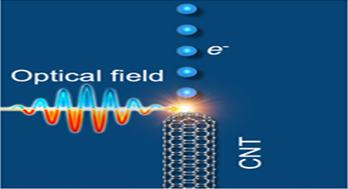
At present, there are two mechanisms of ultrafast electron source: multiphoton emission (relatively weak light) and light field emission (relatively strong light). The multiphoton emission can obtain a low energy divergence (0.7 eV, Nature 521, 200, 2015). However, due to the photon absorption and conversion process, the angle and time of electron emission are relatively random, so the temporal and spatial coherence of the electron beam is difficult to further improve. In contrast, the outgoing electron pulse driven by the optical field has the advantage of phase synchronization with the optical pulse, and is only emitted at the tip by the collimation modulation of the optical field. In recent years, it has become an important technical path to realize the high spatiotemporal coherent electron source. In the early stage, a research group successfully used a 20nm metal nano tip to realize the emission of electron pulses from the optical field. However, due to the size effect of the tip, the excitation light wavelength and the energy divergence of the emitted electron pulse are mutually restricted. It is found that only when the laser wavelength is greater than 800 nm, can we obtain enough mass dynamic potential to enable electrons to enter the light field driven emission mode, which will lead to the energy divergence of outgoing electrons greater than 30 eV (Nature 483, 190, 2012), which is far behind the existing electron energy divergence of TEM (<0.7 eV). Therefore, how to further reduce the energy divergence under the light field emission mechanism is a key scientific problem in the field of building high time (attosecond) spatial (emi) coherent electron sources.
In recent years, Qing Dai's research group systematically studied the effects of chirality, surface defects, adsorbed molecules, geometric morphology, arrangement density, modulation voltage and other factors of carbon nanotubes on the performance of electronic sources (Carbon 89,1, 2015; RSC Advances 5, 105111, 2016; IEEE Electron Device Letters 35786, 2014); By designing the boron nitride carbon nanotube heterostructure, the negative impact of surface adsorption on emission performance was effectively avoided, the surface effective work function was reduced, and the probability of electron tunneling was increased (Small 11, 3710, 2015); Clarified the influence of light field on field emission of carbon nanotubes (Applied Physics Letters 104, 113501, 2014, ACS Applied Materials&Interfaces 7, 2452, 2015; Nanoscale 7, 4242, 2015); Based on theoretical analysis of charge transition and transport mechanism, it is proved that carbon nanotubes have excellent photothermal electron emission characteristics (Carbon 96, 641, 2016; Small 14, 18002652018) and significant local optical field enhancement effect (Applied Physics Letters 110, 093105, 2017).
On the basis of the above, Qing Dai's research team took the lead in proposing the research idea of using carbon nanotubes to replace metal nano needles, and using its structure and energy band advantages to achieve low energy dispersion light field driven electronic pulse, and made a series of progress: first, special single-walled carbon nanotubes were prepared by using the characteristic growth process to obtain an order of magnitude optical field enhancement factor, breaking through the bottleneck of insufficient mass power potential at the emission tip before, For the first time, electron emission in the optical field is realized by using a visible laser. By optimizing the structure of carbon nanotubes, the femtosecond electron emission with the lowest energy divergence of 0.25 eV is obtained, which meets the requirements of atomic level resolution for electron beam energy divergence (<0.7 eV). (Advanced Materials 2917015802017, cover article). Compared with metal tips, carbon nanotubes not only have a hollow structure, which can greatly reduce the electron backscattering effect, but also its quantized band structure (Van Hoof Singularity) provides more possibilities for the control of electron emission in the light field. Through in-depth research, it is found that the use of semiconducting carbon nanotubes can achieve the 40th order extreme nonlinear photoelectron emission, and the optical phase modulation performance is 5 times higher than that of metals, approaching the theoretical limit (the phase modulation depth reaches 100%). This achievement was published online by Nature Communications magazine on October 25, 2019 under the title of "Extreme non-linear strong field photoemission from carbon nanotubes"(https://doi.org/10.1038/s41467-019-12797-z ).
This series of research has been supported by the national key research and development plan of the Ministry of Science and Technology (2016YFA0202000), the major instrument development project of the National Natural Science Foundation of China (11427808), the key deployment project of the Chinese Academy of Sciences (ZDBS-SSW-JSC002), the cross innovation team of the Chinese Academy of Sciences (JCTD-2018-03) and other projects, which has provided help for the use of new nano materials to achieve atomic level time-space resolution electronic sources.

无上一篇
Final acceptance of the National Key Scientific Research Instrument Development
Contact us
Tel:010-82545609
E-mail:qinyl@nanoctr.cn
Add:No.11 ZhongGuanCun BeiYiTiao, 100190 Beijing, P.R. China
Copyright ©2020 国家纳米科技中心 Designed By Mfweb 京ICP备15053254 Website Statement | Privacy Policy